[Infostock Daily= Senior Reporter Lee Hyung-jin and Lee Dong-hee] Samsung Electronics is preparing a semiconductor factory dedicated to EUV (extreme ultraviolet and exposure equipment), which is a state-of-the-art process.
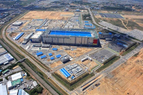
According to Samsung Electronics and related industries on May 24, Samsung Electronics recently confirmed plans to start construction of a semiconductor plant dedicated to EUV at the P3 plant site of Samsung Electronics Pyeongtaek Campus in May.
EUV is a facility that forms light semiconductor circuits on wafers, which are materials for semiconductors. It is currently the only production company in ASML, a Dutch semiconductor equipment company. The unit price per unit is 150 billion ~ 200 billion won, and EUV is essential for microprocessing of 10 nanometers or less.
Samsung Electronics Pyeongtaek Campus, which will have a semiconductor production plant dedicated to EUV, has a P1 plant and a P2 plant.
NAND flash is produced on the first floor of the P1 plant, and DRAM and NAND flash are simultaneously produced on the second floor of the plant.
In addition, the P2 plant is undergoing production facilities from the beginning of this year, and plans to produce NAND flash and DRAM from the second half of this year.
Samsung Electronics has denied expanding its semiconductor plant for the EUV process. An official at Samsung Electronics said, "We know that the P3 plant is not an easy matter to decide because of its large investment."
Senior Reporter Lee Hyung-jin, magicbullet@infostock.co.kr
Reporter Lee Dong-hee, nice1220@infostock.co.kr